3.1 Effect of Laser Wavelength on Processing Polycrystalline Silicon Wafers
The varying effects of different laser wavelengths on the final texture of polycrystalline silicon wafers can be explained by the fact that other parameters must remain constant when using different wavelengths to etch the material's surface. For lasers with wavelengths ranging from 1064 nm to 355 nm, the damage threshold and light penetration depth of polysilicon decrease as the wavelength shortens. Additionally, with shorter wavelengths, the energy is primarily deposited in a very shallow surface layer. As the wavelength decreases, the absorption coefficient of polycrystalline silicon increases, making short-wavelength lasers more likely to ablate the material under the same energy density. At a wavelength of 532 nm, polycrystalline silicon experiences the maximum degree of melting, while at 1064 nm, the melting is minimal, and at 355 nm, it is the least.
Currently, based on the reviewed literature, most studies use infrared lasers with a wavelength of 1064 nm for texturing, while green and ultraviolet lasers are primarily employed in theoretical research. This may be because, although green and ultraviolet lasers, generated by frequency doubling of infrared wavelengths, produce fine processing results, the efficiency of light conversion is significantly reduced, making them less suitable for industrial production. Therefore, when selecting lasers with different wavelengths, both processing performance and factors like efficiency and cost should be considered.
3.2 Effect of Pulsed Laser Spot Spacing in Various Directions on Polycrystalline Silicon Surface Texturing

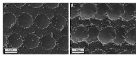
Figure 7 Morphology of overlapping holes formed by adjusting pulse laser parameters
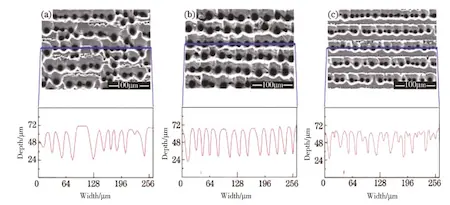
Radfar and others used a nanosecond infrared laser with an output power of 30 W to texture the surface of polycrystalline silicon wafers. They varied the frequency (30 kHz / 55 kHz) to adjust the spot overlap rate (72% / 82%) and observed the resulting morphological changes in the overlapping holes formed on the silicon surface. The optimal reflectivity was found when the repetition frequency was 55 kHz and the overlap rate was 82%. Tiandai Jia and studied the effect of spot spacing on the reflectivity of textured surfaces. They developed a theoretical model using the finite difference time domain (FDTD) method, simulating the interaction between incident light with a wavelength of 700nm and the holes, and determined that the optimal array hole pitch was 30μm. They then used a laser with a wavelength of 515nm, a focused spot diameter of 30μm, and a pulse width of less than 15ps to conduct single-point drilling experiments on the polycrystalline silicon wafer surface. The etched images showed hole spacings of 30μm, 40μm, 50μm, and 60μm (Figure 8). They compared the morphology of array holes with different hole spacings and their surface reflectance in the wavelength range of 350–1050nm under these processing parameters. The results showed that a hole pitch of 30μm produced the optimal processing distance, with a microstructure that effectively reduced the surface reflectivity of polysilicon and improved the photoelectric conversion efficiency of polysilicon solar cells.
Figure 8 The surface of multi-grade silicon samples etched by laser under different hole spacing and the corresponding quilt surface
Xiaozhan Lu and colleagues studied the effects of scanning path spacing and the number of scans on polycrystalline silicon surface texturing. They used a picosecond laser with a pulse width of less than 20ps and a wavelength of 1064nm to process polycrystalline silicon wafers. The laser scanning path spacing was set to a series of closely packed straight lines, with spacings of 20μm, 30μm, and 40μm, as shown in Figure 9. When the scanning spacing was 30μm, relatively uniform and regular hole diameters and depths were achieved. Based on this spacing, they also studied the impact of varying the number of scans (20, 60, 85, and 140) on texturing. With a scanning spacing of 30μm and 85 single-line scans, the texture quality was good, with micropores evenly and densely distributed. No fused residue or cracks were observed around the holes or in the surrounding area, providing a solid foundation for subsequent chemical etching. The primary goal of adjusting micropore spacing is to create a more uniform and light-trapping pit texture on the polycrystalline silicon wafer. As shown in Table 2, by adjusting the spacing between different types of holes, the density of pits per unit area is also altered. Research on light reflection from polycrystalline silicon surfaces has demonstrated that pit density is a key factor influencing the light-trapping properties of the surface.

Figure 9 Microscopic morphology of laser scanned samples under different scanning spacings
Table 2 Effect of spot spacing in different directions on the light absorption properties of multi-crystalline silicon wafers
| Source | Overlap Hole (Spot Overlap Rate, %) | Array Hole (Hole Spacing, µm) | Scanning Pitch Holes (Scanning Path Spacing, µm) | Reflectivity (%) | Reflectivity After Chemical Etching (%) |
| Radfar and others | 82 | — | — | — | 6.59 |
| Tiandai Jia and others | — | 30 | — | 5.17 | 6.95 |
| Xiaozhan Lu and others | — | — | 30 | About 8 | <5 |
Note: "—" means that this content is not indicated in the literature.
3.3 The Influence of Parameters such as Beam Incident Angle, Energy Distribution, and Pulse Width on Polycrystalline Silicon Surface Texturing

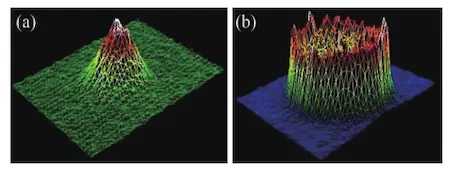
Figure 10 (a) Gaussian beam profile and (b) flat-top beam profile energy distribution