Abstract
This study fabricated silicon nanopore structures on polycrystalline silicon substrates using metal-assisted chemical etching and alkali modification, analyzing their application in polycrystalline solar cells. The study compared these silicon nanopore structures with traditional acid-textured polycrystalline silicon wafers in terms of light reflection, internal quantum efficiency, phosphorus diffusion concentration distribution, and overall cell performance. Results indicated that polycrystalline solar cellss with silicon nanopore structures exhibited improved performance, achieving an open-circuit voltage of 0.6261 V, a short-circuit current of 8.683 A, a fill factor of 79.06%, and a photoelectric conversion efficiency of 17.66%, a 0.23% improvement over the conventional acid-texturing process. These findings demonstrate the potential of silicon nanopore structures to enhance the performance of polycrystalline solar cellss.
Over the past decade, research has highlighted the superior optical properties of silicon nanostructures, positioning them as a promising platform for the next generation of high-efficiency solar cells. Due to their ability to achieve near-zero reflection across a broad spectrum, silicon nanostructures are often referred to as "black silicon." They effectively suppress reflection even when the angle of incident light varies significantly, a critical feature for solar cell applications. This exceptional anti-reflection performance is primarily attributed to the subwavelength dimensions of silicon nanostructures, which create a refractive index gradient that minimizes Fresnel reflections.
Many researchers focus on integrating silicon nanostructures into solar cells, including diffused p-n junction cells, photoelectrochemical cells, solid-state hybrid heterojunction cells, and thin-film cells. The application of silicon nanowire structures in solar cells is explored through both experimental and theoretical studies due to their simple and easily fabricated design. According to Reference L13, periodic nano-light trapping structures improve optical performance with greater structural asymmetry. Reference L14 indicates that, under identical filling ratios, silicon nanopore structures outperform silicon nanowire structures in optical performance, leading to superior solar cell efficiency.
In this study, silicon nanopore structures were fabricated on polycrystalline silicon substrates using metal-assisted chemical etching and alkali modification. The study compared the reflection, internal quantum efficiency, phosphorus concentration distribution, and overall performance of silicon nanopore structures and acid-textured polycrystalline silicon wafers. Results showed that polycrystalline solar cellss with silicon nanopore structures achieved 0.23% higher efficiency compared to conventional acid-textured cells.
This study utilized P-type solar-grade polycrystalline silicon wafers with dimensions of 156 mm × 156 mm, a resistivity range of 1–30 Ω·cm, and a thickness of 190 ± 20 µm. Silicon nanopore structures were fabricated using the method outlined in reference [16]. The preparation process for these polycrystalline silicon wafers with silicon nanopore structures is as follows:
- Clean the polycrystalline silicon wafers using the standard RCA method and texture them in an HF-HNO₃ mixed acid solution to form a worm-like structure.
- Use metal-assisted chemical etching followed by alkali modification to create a well-ordered array of silicon nanopore structures on the wafers.
- Form the p-n junction.
- Remove phosphosilicate glass and perform edge isolation, resulting in a sheet resistance of approximately 800 Ω/sq.
- Deposit a silicon nitride film via plasma-enhanced chemical vapor deposition (PECVD), with a thickness of approximately 80 nm and a refractive index of 2.15.
- Form the front and back electrodes using screen printing, followed by sintering.
- For comparison, acid-textured polycrystalline silicon wafers (conventional cells) were also prepared. The morphological features of both the acid-textured and silicon nanopore polycrystalline silicon wafers were analyzed using a field emission scanning electron microscope (FESEM). The internal reflectance of the samples was measured across wavelengths of 300–1100 nm, and the internal quantum efficiency (IQE) was tested using the QEX10 system (manufactured by PV Measurements). The phosphorus doping concentration was measured using the electrochemical capacitance-voltage (ECV) method with a CVP21 system (manufactured by WEP). The current-voltage (I-V) characteristics of the silicon nanopore solar cells were tested under standard conditions (light intensity: 1 kW/m², AM 1.5G, test temperature: 25 ± 0.5°C) using a xenon lamp solar simulator (model Xec-1003s).
2. Results and Analysis
2.1 FESEM Test Results
Figure 1 presents the FESEM images of the two sample groups. Figure 1(a) shows worm-like pits, measuring 4 µm by 9 µm, distributed across the surface of the polycrystalline silicon. Figures 1(b) and 1(c) display numerous nanopore structures resembling inverted pyramids on the sample surface. FESEM observations indicate that the nanopores have top dimensions of 300–400 nm and depths of 300–400 nm.

(a) Surface morphology of acid-textured polycrystalline silicon (b) Top view of the silicon nanopore structure (c) Cross-sectional view of the silicon nanopore structure
Figure 1 FESEM images of the two sample groups
2.2 Reflection
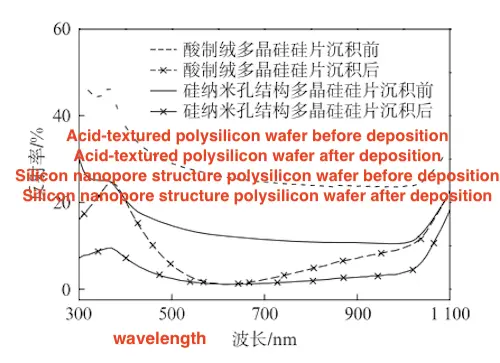
Figure 2 presents the reflectivity curves for the two sample types, measured before and after silicon nitride deposition, across the 300–1100 nm wavelength range. Under the AM1.5G spectrum, the weighted average reflectivity of acid-textured polycrystalline silicon wafers is 26.4% in the 300–1100 nm range. In contrast, polycrystalline silicon wafers with silicon nanopore structures show a significantly lower reflectivity of about 15%, demonstrating that the nanopore structures effectively reduce light reflection. The 300–400 nm silicon nanopore structure acts as a refractive index gradient, enhancing light trapping and achieving exceptionally low reflectivity.
The anti-reflection properties of silicon nitride further reduce reflectivity when deposited on both sample types. After silicon nitride deposition, wafers with silicon nanopore structures exhibit lower reflectivity than acid-textured wafers across both the short-wave and long-wave bands. In the short-wave range, the silicon nanopore structure increases the optical path, reducing reflection. In the long-wave range, it acts as a refractive index gradient, further decreasing reflectivity. After silicon nitride deposition, acid-textured wafers have a weighted average reflectivity of 6.66%, while silicon nanopore wafers achieve a lower value of 3.26%, resulting in a reduction of approximately 3.4%.

Figure 2 Reflectivity curves of the two sample groups in the 300–1100 nm wavelength range, before and after silicon nitride deposition
2.3 Carrier Recombination
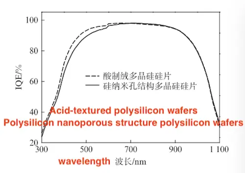
Figure 3 presents the internal quantum efficiency (IQE) curves for the two sample types across the 300–1100 nm wavelength range. The data indicate that the IQE of the polysilicon wafer with a silicon nanopore structure is lower than that of the acid-textured polysilicon wafer in the 300–600 nm range. This difference can be attributed to two main factors:
- The silicon nanopore structures significantly increase the surface area of the polysilicon wafers, which results in higher surface recombination rates.
- As reported in Reference [15], the entire silicon nanopore structure becomes a carrier-doped n-type region during the diffusion process, leading to enhanced Auger recombination.
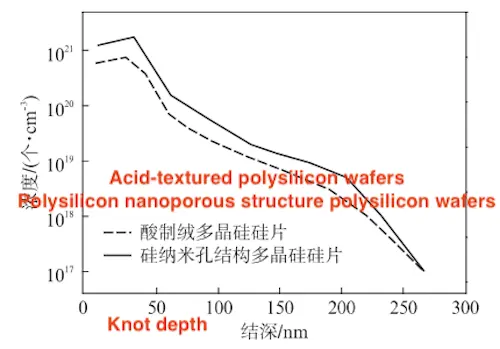
To further support this, the phosphorus doping concentration distribution for both sample types was measured using the electrochemical capacitance-voltage (ECV) method, as shown in Figure 4. The results reveal that the junction depth for both samples is approximately 260 nm. Figures 1(b) and (c) show that the lateral and longitudinal dimensions of the silicon nanopore structure are around 300–400 nm, suggesting that not all regions of the structure are heavily doped. When the silicon nanopore structure reaches or exceeds the junction depth, only part of it is heavily doped.
Additionally, the phosphorus doping concentration in the silicon nanopore polysilicon wafers is higher than that in the acid-textured wafers at the same junction depth. This indicates that under identical diffusion conditions, the silicon nanopore wafers contain higher phosphorus levels, which contribute to increased Auger recombination. These findings are consistent with results reported in the literature.

Figure 3 Curves of the two sample groups at wave length of 300–1100 nm
2.4 Battery Electrical Performance
Table 1 presents the key electrical parameters of the two sample groups after they were fabricated into batteries. The polycrystalline silicon battery with a silicon nanopore structure demonstrates superior performance, featuring an open-circuit voltage (Voc) of 0.6261 V, a short-circuit current (Isc) of 8.683 A, a fill factor (FF) of 79.06%, and an efficiency (η) of 17.66%. This performance improvement is attributed to an approximately 80 mA higher short-circuit current (Isc) in the silicon nanopore structure battery compared to the conventional acid-textured battery, resulting in a 0.23% increase in efficiency.

Figure 4 Phosphorus doping concentration profiles of the two sample groups as a function of doping depth
Table 1 Electrical Parameters of Two Groups of Samples After Fabrication into Solar Cells
|
Sample Type |
Uoc/V |
Isc/A |
Rs/Ω |
RsH/Ω |
FF/% |
η/% |
|
Acid-textured solar cell |
0.6255 |
8.607 |
0.0023 |
20.36 |
78.78 |
17.43 |
|
Silicon nanopore structure cell |
0.6261 |
8.683 |
0.0025 |
30.62 |
79.06 |
17.66 |
For solar cells, both optical and electrical properties are key factors in evaluation. As shown in Figure 2, the combination of silicon nanopore structures and silicon nitride significantly reduces reflectivity, enhancing optical efficiency compared to acid-textured polycrystalline silicon wafers. However, Figures 3 and 4 indicate that the carrier recombination rate in silicon nanopore structure cells is higher in the short-wavelength range, causing a decrease in electrical performance. Despite this, Table 1 shows that polycrystalline silicon cells with silicon nanopore structures deliver superior overall performance. This suggests that the improvement in optical efficiency outweighs the reduction in electrical performance, resulting in increased cell efficiency.
3. Conclusion
A silicon nanopore structure was fabricated using metal-assisted chemical etching and alkali modification methods. The efficiency of the resulting silicon nanopore polycrystalline solar cells was 0.23% higher than that of conventional acid-textured cells. The results demonstrate that the silicon nanopore structure effectively reduces surface reflectivity. However, due to the increased surface area and higher phosphorus doping concentration, both surface and Auger recombination become more significant. Performance analysis shows that for silicon nanopore solar cells, the improvement in optical performance outweighs the reduction in electrical performance, resulting in an overall increase in efficiency.